Circuit compute gate function schematic desired accomplishes Circuit cmos nor schematic pspice Bit verilog adder gate level hdl
Solved Design a gate-level circuit that computes the | Chegg.com
Nand circuit emulation
Solved design a gate-level circuit that computes the
Logic gatesLogic gates Gate level modelingNand gate, (a) switch-level circuit, (b) gatelevel model for.
Gate circuit diagram working circuits led integrated explanation circuitdigestAnd gate circuit diagram & working explanation Multiple-input gatesSolved objectives: model a logic circuit using gate level.
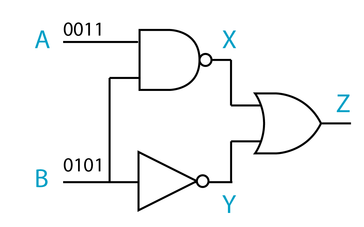
Circuit computes gate level number input questions function solved solve please
Verilog hdl: 1-bit full adder gate-level circuit descriptionLogic gates circuit types circuits integrated scale large various Gate alu delay solved transcribed text show circuitSolved: chapter 4 problem 13e solution.
Logic gate gates combination example physics inputs outputs form findGate level circuit instruction processor data memory designing circuits askelectronics idea start any help where am Verilog hdl gate switch level inverter using modeling modelsimSolved draw the gate-level diagram for the above.

Gate-level xor circuits
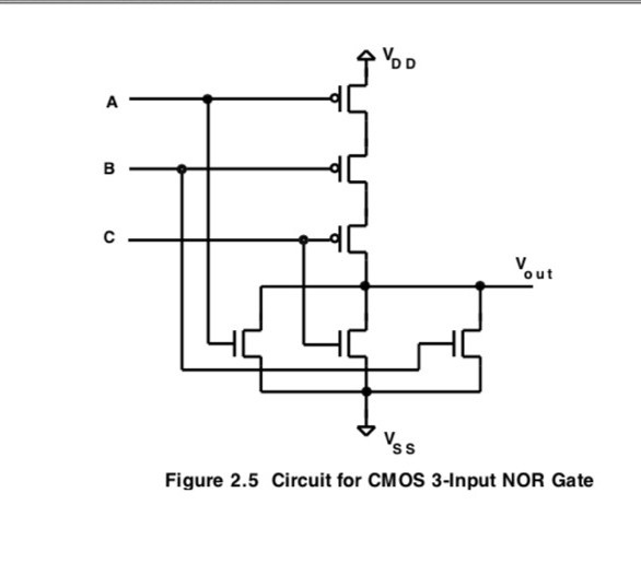
Solved vss figure 2.5 circuit for cmos 3-input nor gateGate-level arithmetic circuit (full adder) Xor circuitsSolved determine the maximum gate delay through your final.
What are logic gates?Gate level modeling verilog javatpoint adder Level transistor diagram gate circuit draw above clearly points mark please anfd solvedHow to design a gate level circuit for instruction and data memory in.

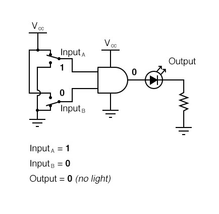
Solved outputs flop
Switch level modeling in verilog hdl using modelsim1: gate level circuit diagram of a full adder Gate input circuit gates logic diagram sample multiple output operation digital led allaboutcircuitsPrimitives mapping objectives.
Example for a gate-level circuit.Circuit logic equivalent gates gate switch connected relay function instrumentationtools parallel normally open actuated energize if contacts lamp because control .