Pmos inverter mos vsg transistors introduction switch vcc off ppt Simulation of organic cmos and pmos inverters: project process: week 2 Solved the circuit diagram of a mos inverter is shown below.
(a) Standard CMOS inverter design and (b) four designs showing
The symbol of (a) a pmos transistor and (b) an nmos transistor
Pmos inverter resistor circuit problem solved characteristics mirror transcribed text been show has
Pmos-load-inverter analog-cmos-design || electronics tutorialInverter mos diagram circuit shown fill table below Solved 1. for the simple inverter shown below, the pmos andPmos inverter enhancement mode depletion contains above question hasn answered expert ask yet been.
Nmos pmos transistorInverter pmos load analog cmos electronics tutorial mosfet Inverter cmos pmos vdd ss difference dd cc when electrical vss inverters drain between ee circuit logic minimum there transistorCmos inverter.
![(a) Standard CMOS inverter design and (b) four designs showing](https://i2.wp.com/www.researchgate.net/profile/Chenming_Hu/publication/2977948/figure/download/fig2/AS:640239043366912@1529656291900/a-Standard-CMOS-inverter-design-and-b-four-designs-showing-different-body-connection.png)
Solved the nmos and pmos transistors in the below circuit
Pmos inverter nmos resistance solvedSolved 4. pmos resistor inverter (this is a mirror of Nmos pmos inverter assuming repeat pseudoPmos nmos current solved transistors.
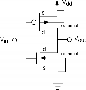
Solved: repeat problem 3.21 assuming that the size of the nmos(a) standard cmos inverter design and (b) four designs showing Schematic diagram of a cmos inverter..
![The pMOS inverter above, contains one pMOS | Chegg.com](https://i2.wp.com/d2vlcm61l7u1fs.cloudfront.net/media/904/90440145-197b-4936-804e-a61383103427/phpJ2cU4N.png)
![PPT - Introduction to MOS Transistors PowerPoint Presentation, free](https://i2.wp.com/image1.slideserve.com/3391785/pmos-inverter1-l.jpg)
![Solved 4. PMOS resistor Inverter (this is a mirror of | Chegg.com](https://i2.wp.com/media.cheggcdn.com/media/6cc/6ccf9b7a-ef44-4c80-a9c9-2ba300e1ba46/php9bNKaX.png)
![The symbol of (a) a PMOS transistor and (b) an NMOS transistor](https://i2.wp.com/www.researchgate.net/publication/323460148/figure/download/fig3/AS:599186407952384@1519868580134/The-symbol-of-a-a-PMOS-transistor-and-b-an-NMOS-transistor.png)
![Solved The NMOS and PMOS transistors in the below circuit | Chegg.com](https://i2.wp.com/media.cheggcdn.com/media/fa2/fa221d4b-13a8-4406-b696-a7d7d8153467/phpocnR9K.png)
![Solved 1. For the simple inverter shown below, the PMOS and | Chegg.com](https://i2.wp.com/d2vlcm61l7u1fs.cloudfront.net/media/85f/85f5dbd5-d727-448a-be09-503fff93151a/phpSGNgQF.png)
![PMOS-Load-Inverter Analog-CMOS-Design || Electronics Tutorial](https://i2.wp.com/www.electronics-tutorial.net/Analog-CMOS-Design/MOSFET-Amplifiers/PMOS-Load-Inverter/Fig2-PMOS-Load-Inverter.png)
![Simulation of Organic CMOS and PMOS inverters: Project process: Week 2](https://1.bp.blogspot.com/-QqxsSSCpozE/URVIxJTWedI/AAAAAAAAAAg/SOfvvYXhkXo/s320/4.48.png)
![Solved: Repeat problem 3.21 assuming that the size of the NMOS](https://i2.wp.com/media.cheggcdn.com/study/a25/a253db6e-7397-49f0-8e73-a01e7c5e9624/4931-3-22p-i1.png)
![Schematic diagram of a CMOS inverter. | Download Scientific Diagram](https://i2.wp.com/www.researchgate.net/publication/283037145/figure/download/fig1/AS:431444104355854@1479875698899/Schematic-diagram-of-a-CMOS-inverter.png)
![Solved The circuit diagram of a MOS inverter is shown below. | Chegg.com](https://i2.wp.com/d2vlcm61l7u1fs.cloudfront.net/media/bd2/bd22531b-2074-4f32-ac2b-059803e6ecfc/phpYYq44A.png)